Ready to Source Your Actuator-Grade Wafers?
Whether you’re developing MEMS comb-drives, piezoelectric thin-films, or photonic actuators, we can provide SOI, LiNbO3, and PZT/AlN wafers in research and production quantities. Upload your specs or request a quote today.
Need precision wafers for your next MEMS project?
Order SOI, LiNbO₃, and PZT/AlN wafers engineered for actuator performance — order now or request a custom quote.
Get Your Quote FAST! Or, Buy Online and Start Researching Today!
Get a Fast Quote
- Silicon & SOI wafers for comb-drives, flexures, and MEMS mirrors
- PZT, AlN, and AlScN piezo films on Si/SOI or membranes
- LiNbO3 wafers for SAW/BAW and photonic actuation
- Quartz, Sapphire, GaN, and SiC available on request
Research & production quantities • Global shipping • Fast turnaround
Popular Substrates
- SOI — Ideal for DRIE combs and stable flexures.
- Prime Si — Used for caps, carriers, and support wafers.
- LiNbO3 — Strong piezo & electro-optic effects.
- Quartz/Sapphire — High thermal stability & optical clarity.
When to Choose Each
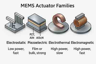
- Electrostatic — Fast, low power, high voltage, small stroke.
- Piezoelectric — High precision and force, CMOS-compatible options.
- Electrothermal — Large stroke, slower actuation, more power.
- Electromagnetic — High force, coil and magnet design dependent.
Designing Actuators with the Right Wafer Stack
UniversityWafer supports actuator R&D across electrostatic, piezoelectric, electrothermal, and electromagnetic designs. Start with Silicon/SOI for high-aspect micromechanics, add thin-film piezo stacks (PZT, AlN/AlScN), or select LiNbO3 for SAW/BAW and photonic tuning. Applications include micro-positioners, MEMS mirrors, RF/acoustic devices, and precision opto-mechanics.
Core Mechanisms
Electrostatic (Comb-Drives, Plates)
Voltage-induced attraction between interdigitated fingers or plates. Advantages: fast dynamics, low static power, excellent CMOS integration. SOI is ideal for tall combs and stable gaps; DRIE defines fingers and flexures.
Piezoelectric (PZT, AlN/AlScN, LiNbO3)
Electric field causes film/crystal strain for force and displacement. PZT gives large coefficients (lower drive voltage for a given force); AlN/AlScN favors CMOS flows and low RF loss; LiNbO3 enables SAW/BAW and electro-optic actuation.
Electrothermal
Resistive heating of beams → thermal expansion → big stroke and force; manage power and thermal time constants.
Electromagnetic
Lorentz forces from on-chip coils or integrated magnets; strong forces but package/coil design dominates.
Recommended Wafer Options
- SOI (device 10–100 µm, BOX 1–3 µm): deep combs, mirrors, robust anchors.
- Prime Si (DSP/SSP): caps, frames, membranes, carriers.
- LiNbO3 (128°Y-X, Z-cut, etc.): SAW/BAW and piezo-MEMS actuators.
- PZT / AlN / AlScN films on Si or SiN membranes with metal electrodes.
- Quartz / Sapphire: stable optics/RF substrates; dielectric/thermal advantages.
Fabrication Notes
- DRIE (Bosch/cryogenic) for high-aspect combs and trenches; manage footing and lag with masks/recipes.
- Thin-film piezo via sputter/PLD/sol-gel; sandwich between electrodes; pattern with liftoff/etch.
- Release on SOI via HF of BOX; dimples/stoppers mitigate stiction.
- Packaging can change dynamics (magnetic fields, heat sinking, acoustic loading).
Quick Selection Guide
| Goal | Best Starting Point | Why |
|---|---|---|
| Fast & low power scanning | SOI + comb-drive | High-Q flexures; simple drive; CMOS-friendly |
| High force & bandwidth | PZT thin-film on Si/SOI | Large piezo coefficients → force at modest V |
| RF/SAW/optic tuning | LiNbO3 wafer | Strong piezo & electro-optic properties |
| Large stroke micro-positioner | Electrothermal beams | Thermal expansion yields big travel |