LiNbO3 Substrate for Research & Development
Lithium niobate (LiNbO3) is a high-performance electro-optic and piezoelectric crystal widely used in SAW filters, modulators, acousto-optic components, and integrated photonic devices. This page explains the key material properties that make LiNbO3 valuable, how crystal orientation and wafer cut influence performance, and what substrate specs researchers typically define when selecting LiNbO3 wafers for device fabrication and characterization.
SAW Properties of LiNbO3 Substrates
A graduate student requested a quote for the following.
I wanted to know the SAW velocity for the following Lithium Niobate wafer. Can you kindly share the data-sheet regarding the SAW properties of these wafers.
- LiNbO3 Wafer
- 55x40x1.0mm
- 128-Y cut
- SAW Grade X parallel to 55mm long side
Double side polished.
Reference #245914 for specs and pricing.
Lithium Niobate (LiNbO3)
LiNbO3 is a useful material for optoelectronics, and many technologies are based on the fact that the material has unique piezoelectrostatic, optical and photoelastic properties, while maintaining mechanical and chemical stability. This makes it attractive for use in integrated optics and as a material of great interest in the field of photonics.
Lithium Niobate (LiNbO3) Wafers
Lithium niobate (LiNbO3 or LN) is an optical material that is well supported and widely used.
LiNbO3 crystals can be found in the following industries:
- Electro-optics
- Acousto-optics
- Nonlinear optics
- Guided-wave optics
Get Your Quote FAST! Or, Buy Online and Start Researching Today!
What Does Lithium Niobate Substrate Look Like?
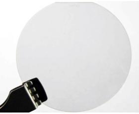
LiNbO3 Beneficial Properties:
- Wide transparency range
- high electro-optic and nonlinear optic coefficients
- very high electro-mechanical coupling coefficients
- chemical and mechanical stability
Our inventory includes a large selection of dimensions and diameters as well as thicknesses and other specs.
Please contact us today for an immediate quote.
Optical Grade Lithium Niobate
This material was developed as a next generation material by the University of California, San Diego Department of Materials Science and Engineering (DMSE).
The main application is the production of high-performance, cost-effective and high-performance electronic devices. In the case of subgrain and lead-free wafers, damage caused by magnesium doping leads to contamination of the material with lead, lead oxide and lead-containing materials.
Add to this the high cost of lead-free wafers and the lack of a high-quality, cost-effective alternative for the production of electronic devices.
Lithium Niobate Saw Applications
The most commonly used orientation is the YZ (128Adeg) cut, which is best suited for high-end laser cutters such as the MOSFET and XMOS.
Accordingly, the dual-power rotating wafers 171Adeg and 106ADeg have shown increasing interest. The ability to rotate sections at high speed without sound is of growing demand for applications for high-speed sound processing.
What are LiNbO3 Advantages
Lithium niobate modulators are used in digital communications networks and wireless networking  devices. They are used in radar detection systems for detecting unknown aircraft. They are relatively inexpensive compared to other materials and are suitable for a wide variety of applications. Another advantage of lithium niobate is its high dispersion, making it well-suited for optical modulation. And, thanks to their low residual birefringence, they are ideal for use in telecommunications.
Another advantage of Lithium Niobate is its ability to perform modulation at extremely high speeds. This feature makes it a viable choice in wireless LAN networks. Because of its unique characteristics, lithium niobate has high sensitivity and is resistant to cross-modulation. Its low sensitivity to noise and distortions makes it ideal for telecommunications applications. Despite its disadvantages, lithium niobate is gaining momentum as a promising material for optical modulators.
Other advantages of Lithium Niobate include its ability to be flexible and lightweight. For example, the material's ultrahigh-voltage capacity makes it suitable for wireless applications. Despite its low-power consumption, it can resist electro-magnetic fields. This property makes it ideal for wireless LANs. In addition, the device is resistant to cross-modulation and has high-density transmission.
Related Materials & Resources


 devices. They are used in radar detection systems for detecting unknown aircraft. They are relatively inexpensive compared to other materials and are suitable for a wide variety of applications. Another advantage of lithium niobate is its high dispersion, making it well-suited for optical modulation. And, thanks to their low residual birefringence, they are ideal for use in telecommunications.