
Your project deserves the right wafer. Ask our engineers which specs fit best.
Call now: 1-800-713-9375
Order today and receive a free consultation from our experts.
SOI Quick Facts
- Three-layer design: Handle wafer, Buried Oxide (BOX), Device Layer
- Reduces parasitic capacitance → faster switching
- Consumes 20–50% less dynamic power than bulk CMOS
- Provides inherent radiation hardness for aerospace/defense
FDSOI vs PDSOI
- FDSOI: Ultra-thin device layer (≤50 nm), full depletion, best for low-power, mobile & IoT
- PDSOI: Thicker device layer (100–200 nm), high drive current, ideal for analog, RF, and HPC
Manufacturing Highlights
- SIMOX: Ion implantation + high-temp annealing to form BOX
- Wafer Bonding: Smart Cut™, Direct Bonding, and layer transfer methods
- Modern processes achieve ±5% BOX uniformity across 300 mm wafers
Key Benefits for ICs
- Up to 30% faster switching
- Elimination of latch-up failures
- Reduced leakage → longer battery life
- Lower operating voltages down to 0.7 V
- Better RF isolation and less cross-talk
Application Domains
- CMOS Logic: Scalable, low-power processors
- RF Circuits: Lower insertion loss, high Q passives
- MEMS: BOX as an etch-stop, reliable micromachining
- Photonics: SOI waveguides for optical communications
- Defense & Space: Radiation-hard, thermally stable ICs
Emerging Research
- Quantum: SOI spin qubits & cryogenic CMOS
- Neuromorphic: SOI synaptic devices for AI at the edge
- Power Electronics: SOI MOSFETs for DC-DC converters
Explore More
Applications of Silicon-On-Insulator in Integrated Circuits
Key Takeaways
- Silicon-On-Insulator (SOI) technology provides better electrical isolation and reduced power consumption compared to standard silicon wafers
- SOI wafers feature a three-layer structure: handle wafer, buried oxide layer, and device layer
- Major applications include CMOS technology, MEMS devices, and photonics integration
- Manufacturing methods include SIMOX (Separation by Implantation of Oxygen) and wafer bonding techniques
- SOI technology enables high-performance integrated circuits with reduced parasitic capacitance and improved scaling
- Applications span from consumer electronics to aerospace and military systems
- Fully Depleted SOI (FDSOI) offers superior subthreshold performance for ultra-low power applications
- SOI provides inherent radiation hardness, making it ideal for space and nuclear applications
- Silicon photonics on SOI enables next-generation optical communication systems
- Advanced SOI manufacturing techniques continue to reduce costs and improve device layer uniformity
Introduction to Silicon-On-Insulator Technology
Silicon-On-Insulator (SOI) technology is one of the biggest advances in semiconductor manufacturing in recent decades. Unlike regular silicon wafers, SOI wafers have a special structure with a thin layer of silicon on top of an insulating material, usually silicon dioxide (SiO₂). This simple change creates big improvements in how integrated circuits perform by changing how electrons move within semiconductor devices and reducing unwanted effects that limit normal silicon technologies.
The main advantage of SOI technology is that it electrically isolates the active device region from the substrate below. This isolation reduces parasitic capacitances and eliminates many problems found in conventional bulk silicon devices, including latch-up susceptibility, junction leakage, and substrate coupling effects. By providing this electrical isolation, SOI technology lets devices work more efficiently, use less power, and perform better across different operating conditions. Our SOI wafer services give researchers and manufacturers access to both bonded and SIMOX SOI technologies, enabling advanced integrated circuit development for applications from high-performance computing to low-power mobile devices.
SOI technology dates back to the 1960s, but it wasn’t until the 1990s that manufacturing techniques became good enough for commercial use. The technology was first developed for radiation-hardened military and aerospace applications, where its natural resistance to radiation effects was a big advantage over conventional silicon. As manufacturing processes improved and costs went down, SOI technology gradually moved into mainstream commercial applications. Today, SOI wafers are key components in many high-performance electronic devices, from mobile processors to radiation-hardened aerospace applications. The technology keeps evolving, with ongoing research focused on thinner device layers, improved insulator materials, and new fabrication techniques to further enhance performance and reduce manufacturing costs for next-generation integrated circuits.
Structure and Types of SOI Wafers
SOI wafers have a special three-layer structure that creates their enhanced performance characteristics. Understanding this structure helps explain how SOI technology enables advanced integrated circuit applications and provides big advantages over conventional bulk silicon technologies.
Basic SOI Structure
The typical SOI wafer consists of:
- Handle Wafer/Substrate – The bottom silicon layer that provides mechanical support and serves as the foundation of the wafer structure. This layer is typically 500-750 μm thick and is made of standard silicon similar to conventional wafers. While not electrically active in most applications, the handle wafer’s properties can be tailored for specific thermal or mechanical requirements.
- Buried Oxide (BOX) Layer – The middle insulating layer, typically silicon dioxide with thicknesses ranging from 100 nm to several micrometers depending on the application. This critical layer provides the electrical isolation that defines SOI technology and determines many of its performance characteristics. The quality and uniformity of this oxide layer significantly impact device performance and reliability.
- Device Layer – The top thin silicon layer where active devices are fabricated, with thicknesses ranging from less than 10 nm to several micrometers depending on the application. The crystalline quality, thickness uniformity, and doping profile of this layer are crucial for device performance and must be precisely controlled during manufacturing.
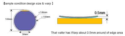
The thickness of each layer can be precisely controlled during manufacturing to optimize for specific applications, with modern fabrication techniques achieving remarkable uniformity across 300mm wafers. The device layer thickness is particularly critical as it determines whether the SOI behaves as fully or partially depleted, significantly affecting electrical characteristics. SIMOX SOI wafers offer unique capabilities for applications requiring high-temperature expansion, making them particularly valuable for specialized integrated circuit designs operating in extreme environments or requiring exceptional thermal stability.
Types of SOI Wafers
SOI wafers are primarily categorized based on the thickness of the device layer and the resulting electrical characteristics, with each type offering distinct advantages for specific applications:
Fully Depleted SOI (FDSOI)
In FDSOI wafers, the device layer is extremely thin (typically less than 50 nm), allowing the depletion region to extend throughout the entire silicon film when the transistor is in operation. This complete depletion of the channel region results in:
- Complete electrical isolation between the source and drain regions, minimizing leakage currents
- Reduced short-channel effects, allowing for better scaling to smaller technology nodes
- Lower threshold voltage variations, improving circuit reliability and performance consistency
- Improved subthreshold swing approaching the theoretical limit of 60mV/decade, enabling lower operating voltages
- Elimination of floating body effects that can complicate circuit design in partially depleted devices
FDSOI technology is particularly beneficial for low-power applications and advanced node technologies where leakage current control is critical, such as mobile processors and Internet of Things (IoT) devices requiring extended battery life.
Partially Depleted SOI (PDSOI)
PDSOI wafers feature a thicker device layer (typically 100-200 nm), where the depletion region does not extend through the entire silicon film during normal operation. This creates:
Our SOI wafer technologies enhance performance in semiconductor devices by reducing parasitic capacitance and improving scaling capabilities, making them ideal for both FDSOI and PDSOI applications across a wide range of integrated circuit designs from high-performance computing to specialized analog/RF systems.
Manufacturing Methods
The two primary methods for manufacturing SOI wafers are:
- SIMOX (Separation by Implantation of Oxygen) – Oxygen ions are implanted into a silicon wafer at a specific depth and then annealed at high temperature (typically above 1300°C) to form a buried oxide layer. This process creates a continuous insulating layer beneath a thin surface layer of single-crystal silicon. SIMOX technology offers excellent uniformity and is particularly suitable for creating very thin device layers.
- Wafer Bonding – Two silicon wafers are bonded together with an oxide layer in between, and then one wafer is thinned to create the device layer. This approach includes several variations such as direct bonding, Smart Cut™ process (which combines bonding with hydrogen implantation for precise splitting), and epitaxial layer transfer techniques. Wafer bonding offers greater flexibility in layer thicknesses and material combinations.
Each manufacturing method offers distinct advantages for specific applications, with SIMOX SOI wafers being particularly valuable for applications requiring high-temperature stability and electrical isolation. The choice between these technologies depends on factors including the required device layer thickness, buried oxide properties, cost considerations, and specific application requirements. Advanced manufacturing techniques continue to evolve, enabling ever more precise control over layer thicknesses and interface properties while reducing costs through improved process efficiency.
Manufacturing Techniques for SOI Wafers
Making high-quality Silicon-On-Insulator wafers involves sophisticated manufacturing processes that have improved greatly over the decades. These techniques are essential for creating the precise layered structure that gives SOI its advantages for integrated circuit applications. Each manufacturing method offers different trade-offs in layer quality, thickness control, cost, and ability to scale to large wafer sizes.
SIMOX Technology (Separation by Implantation of Oxygen)
SIMOX is one of the most established methods for creating SOI wafers and continues to be widely used for specialized applications that require exceptional layer uniformity and high-temperature stability.
The SIMOX process involves:
- Ion Implantation: High-dose oxygen ions (O⁺) are implanted into a silicon wafer at energies typically between 150-200 keV. This implantation process requires specialized high-current implanters capable of delivering doses in the range of 10¹⁷-10¹⁸ ions/cm². The implantation creates a buried layer of oxygen-rich silicon that will eventually form the insulating oxide.
- High-Temperature Annealing: The implanted wafer undergoes annealing at temperatures above 1300°C, often approaching 1350-1400°C, for several hours in an inert or slightly oxidizing atmosphere. This extreme thermal processing causes the implanted oxygen to react with silicon to form a buried silicon dioxide layer while simultaneously repairing crystal damage in the surface silicon layer.
- Surface Refinement: The surface silicon layer is refined to remove remaining implantation damage and create a high-quality device layer. This may involve chemical-mechanical polishing (CMP) and additional thermal treatments to achieve the desired surface quality and thickness uniformity.
SIMOX SOI technology offers several unique advantages:
- Exceptional uniformity of the buried oxide layer across large wafer diameters, with thickness variations typically less than ±5%
- Ability to create very thin device layers with precise thickness control, making it ideal for fully depleted SOI applications
- Excellent high-temperature stability, making these wafers ideal for applications requiring thermal expansion or high-temperature processing
- Superior electrical isolation characteristics with minimal oxide defects and interface traps
- Compatibility with standard semiconductor processing equipment and techniques
As noted in our product information, “SIMOX SOI has unique abilities to expand to very large dimensions, making it useful for applications requiring high temperature expansion.” This property is particularly valuable for integrated circuits operating in extreme environments such as aerospace, automotive under-hood electronics, and industrial systems where thermal stability is critical for reliable operation.
Advantages of SOI Technology in Integrated Circuits
Silicon-On-Insulator technology offers many performance advantages that make it increasingly important for advanced integrated circuit applications. These benefits directly lead to improved device performance, reduced power consumption, and better reliability, making SOI an attractive platform for a wide range of electronic systems from mobile devices to high-performance computing and specialized applications in harsh environments.
Electrical Performance Improvements
Reduced Parasitic Capacitance
One of the biggest advantages of SOI technology is the major reduction in parasitic capacitance. In conventional bulk silicon devices, junction capacitances between the source/drain regions and the substrate limit switching speed and increase power consumption. These parasitic capacitances act as unwanted charge storage elements that must be charged and discharged during each switching cycle, wasting energy and limiting performance. SIMOX SOI wafers eliminate these parasitic capacitances by isolating the active device regions from the substrate with an insulating oxide layer, allowing charge to flow only where it’s needed for device operation.
This reduction in parasitic capacitance delivers:
- Up to 30% faster switching speeds in digital circuits, enabling higher clock frequencies and improved computational performance
- Lower dynamic power consumption, typically 20-50% less than equivalent bulk silicon devices, extending battery life in mobile applications
- Improved high-frequency performance in analog and RF circuits, with higher cutoff frequencies and better linearity
- Enhanced signal integrity with reduced crosstalk between adjacent devices and circuit blocks
- Better performance scaling with decreasing supply voltages, enabling more efficient low-voltage operation
Elimination of Latch-up
Conventional CMOS technologies suffer from a potentially catastrophic failure mechanism called latch-up, where parasitic bipolar transistors form a feedback loop that can cause device failure through excessive current flow. This phenomenon limits circuit design flexibility and requires specific layout rules and guard rings that consume valuable silicon area. The insulating layer in SOI completely eliminates this risk by preventing the formation of these parasitic structures, improving both reliability and design flexibility while enabling higher integration density and simplified circuit layouts.
Reduced Leakage Currents
As noted in our product information, SIMOX wafers offer better electrical isolation and use less power than standard silicon wafers. This improved isolation significantly reduces leakage currents, which is particularly important for low-power applications like mobile devices and IoT sensors where standby power consumption directly impacts battery life. The reduction in leakage currents comes from several mechanisms:
- Elimination of substrate leakage paths through the buried oxide layer
- Reduced junction areas that minimize reverse-bias leakage
- Better control of short-channel effects that contribute to subthreshold leakage
- Improved isolation between adjacent devices that prevents unwanted current paths
Thermal and Radiation Advantages
Radiation Hardness
The insulating layer in SOI wafers provides natural radiation tolerance by:
- Reducing the volume of silicon where radiation-induced charge can be generated, minimizing the impact of particle strikes
- Preventing the collection of radiation-generated carriers from the substrate, which is a major source of soft errors in bulk silicon devices
- Reducing single-event effects by isolating sensitive device regions and limiting charge collection volume
- Reducing total ionizing dose effects through the elimination of parasitic leakage paths that typically degrade with radiation exposure
- Providing better isolation between adjacent devices, preventing radiation-induced cross-talk and interference
This makes SOI technology particularly valuable for aerospace, defense, and nuclear applications where radiation exposure is a concern and device reliability is critical.
CMOS Technology on SOI Platforms
Complementary Metal-Oxide-Semiconductor (CMOS) technology forms the backbone of modern integrated circuits, and its implementation on Silicon-On-Insulator platforms has revolutionized performance capabilities. SOI-based CMOS offers significant advantages over traditional bulk silicon implementations, particularly for high-performance and low-power applications where the unique electrical characteristics of SOI can be leveraged to overcome limitations of conventional approaches.
Fundamental Differences Between Bulk and SOI CMOS
In traditional bulk CMOS, transistors are fabricated directly on a silicon substrate, requiring complex well structures to isolate NMOS and PMOS devices. This approach requires careful management of substrate effects, well biasing, and isolation techniques to prevent unwanted interactions between adjacent devices. In contrast, SOI CMOS benefits from the inherent isolation provided by the buried oxide layer, which fundamentally changes the electrical behavior and integration characteristics of the devices. This fundamental difference creates several key advantages that impact both performance and manufacturability:
- Simplified Device Isolation: The buried oxide eliminates the need for deep well implants and complex isolation structures, reducing process complexity and enabling higher integration density.
- Reduced Junction Capacitance: Source and drain junctions terminate at the insulator rather than forming large capacitive junctions with the substrate, dramatically reducing parasitic capacitances.
- Elimination of Substrate Bias Effects: The isolated device layer prevents substrate noise coupling and bias-dependent performance variations, improving circuit stability and noise immunity.
- Improved Scalability: The superior electrostatic control in SOI devices enables better scaling to smaller technology nodes, with reduced short-channel effects and improved subthreshold characteristics.
SOI CMOS for Low-Power Applications
The power efficiency advantages of SOI CMOS make it particularly valuable for energy-constrained applications where battery life and thermal management are critical concerns:
- Reduced Dynamic Power Consumption: Lower parasitic capacitances translate to reduced switching power, typically 20-50% power savings compared to bulk CMOS.
- Lower Operating Voltages: FDSOI devices can operate efficiently at supply voltages below 0.7V.
- Reduced Leakage Currents: The insulating layer prevents substrate leakage paths, significantly reducing static power consumption.
- Back-Biasing Capabilities: FDSOI allows forward and reverse body biasing to dynamically tune power/performance tradeoffs.
RF and Mixed-Signal Applications
Silicon-On-Insulator technology has become increasingly important for radio frequency (RF) and mixed-signal integrated circuits. The unique properties of SOI wafers address many challenges in these applications, enabling higher levels of integration and performance than conventional bulk silicon technology.
SOI Advantages for RF Circuit Design
- Superior Substrate Isolation: Reduces substrate coupling and crosstalk, enabling high-density integration.
- Reduced Parasitic Capacitances: Improves high-frequency performance and increases cutoff frequencies.
- Higher Quality Passive Components: Enables inductors and capacitors with higher Q-factors.
- Lower Insertion Loss: Transmission lines on SOI exhibit lower losses, especially at millimeter-wave frequencies.
Silicon-on-Sapphire for RF Applications
Silicon-on-Sapphire (SOS) represents a specialized form of SOI technology that offers exceptional RF performance:
- Superior insulation compared to silicon dioxide
- Very high resistivity (>10^14 Ω·cm) for improved passive component performance
- Excellent thermal properties for high-power RF applications
- Enhanced linearity and radiation hardness
MEMS and Sensor Applications
SOI wafers provide unique structural advantages for MEMS fabrication:
- Precision Etch Stop: BOX layer allows highly controlled micromachining.
- Device Layer Isolation: Prevents electrical interference between integrated sensor elements.
- Thermal Isolation: Improves measurement accuracy for temperature-sensitive devices.
- Simplified Release Process: Easier fabrication of movable structures with high yield.
SOI enables integrated sensor systems combining MEMS structures with on-chip signal conditioning and digital processing, creating compact, high-performance smart sensors for IoT, biomedical, and industrial applications.
Photonics Integration on SOI Platforms
Silicon photonics leverages SOI’s high refractive index contrast to build optical waveguides and devices:
- Compact photonic circuits with micron-scale bending radii
- Efficient coupling with fibers and components
- Wavelength-scale devices such as ring resonators and Bragg gratings
- CMOS process compatibility for electronic-photonic integration
Applications include high-speed transceivers, WDM optical networks, 5G infrastructure, and optical interconnects for data centers.
Emerging Applications and Future Trends
Quantum Computing
- SOI quantum dots and spin qubits benefit from excellent electrical isolation.
- SOI devices function well at cryogenic temperatures, enabling integrated quantum control electronics.
Neuromorphic Computing
- SOI enables synaptic devices and analog memory elements.
- Supports low-power edge AI and spiking neural networks.
Advanced Power Management
- High-efficiency DC-DC converters using SOI power transistors
- Energy harvesting circuits for IoT devices
- Wireless power transfer systems leveraging SOI’s high-frequency performance
Conclusion
Silicon-On-Insulator technology is a transformative platform for integrated circuit design, delivering:
- Reduced parasitic capacitance
- Enhanced electrical isolation
- Lower power consumption
- Radiation hardness
- Compatibility with CMOS processes
SOI is now critical for applications ranging from smartphones to satellites. As manufacturing costs decline and performance demands increase, SOI’s role in emerging domains such as quantum computing, neuromorphic systems, and photonics will continue to expand.
UniversityWafer’s SOI wafer solutions support innovation across all these domains, providing high-quality materials and technical expertise to help researchers and manufacturers realize the full potential of SOI technology.