
Get a Quote in Minutes Exclusive discounts for universities & labs.
1-800-713-9375
SOI-MEMS Quick Facts
- Device layer: typically 5–50 μm thick
- Buried oxide (BOX): ~2 μm → acts as etch stop
- DRIE defines high-aspect-ratio MEMS structures
- Main uses: accelerometers, gyroscopes, RF MEMS
- Market: projected 12.8% CAGR growth through 2028
Fabrication Highlights
- DRIE: Vertical sidewalls, BOX as etch stop
- Sacrificial release: BOX removed with HF etch
- Wafer bonding: fusion, anodic, or adhesive for 3D MEMS
Material & Structural Advantages
- Single-crystal device layer → high stiffness & low hysteresis
- BOX ensures electrical isolation & precise etch control
- Mechanical structures maintain integrity over billions of cycles
Applications Beyond Sensors
- RF MEMS: switches, tunable capacitors, resonators
- Optical MEMS: micromirrors, scanners, photonics integration
- Biomedical: implantable sensors, microfluidics, lab-on-chip
Emerging Trends
- Integration with CMOS for complete SoCs
- Use of novel materials (graphene, piezoelectrics) on SOI
- Ultra-thin device layers <100 nm for next-gen MEMS
- Smart MEMS with AI and wireless connectivity
Learn More
Innovative Uses of SOI Technology in MEMS Devices
Essential Points About SOI Technology in MEMS
- SOI wafers reduce parasitic capacitance and improve device performance
- SOI technology enables superior electrical isolation in MEMS devices
- Common applications include accelerometers, gyroscopes, and RF MEMS
- SOI-based MEMS offer advantages in size, power consumption, and reliability
- Device layer thickness typically ranges from 5-50μm with 2μm buried oxide
- Deep Reactive Ion Etching (DRIE) is the primary fabrication method
- SOI enables both sensing and actuation mechanisms in a single device
Key Takeaways
| Performance Benefits | SOI technology significantly reduces parasitic capacitance by up to 80%, resulting in faster switching speeds and lower power consumption in MEMS devices |
| Fabrication Advantages | The buried oxide layer serves as a precise etch stop during DRIE processes, enabling high-aspect-ratio structures with exceptional dimensional control |
| Integration Capabilities | SOI platforms facilitate monolithic integration of MEMS with CMOS electronics, creating complete systems-on-chip with reduced signal path lengths |
| Market Growth | The SOI-MEMS market is projected to grow at 12.8% CAGR through 2028, driven by automotive, consumer electronics, and biomedical applications |
| Future Directions | Emerging trends include ultra-thin device layers below 100nm, integration with AI processing, and incorporation of novel materials like graphene and piezoelectrics |
Introduction to SOI Technology in MEMS Devices
Microelectromechanical systems (MEMS) represent one of the most exciting technological advancements in recent decades. These tiny devices combine electrical and mechanical components at the microscale, enabling functions that were once impossible to achieve in such small packages. At the heart of many cutting-edge MEMS innovations is Silicon-on-Insulator (SOI) technology, which has changed the game for how these miniature devices are designed and built.
SOI wafers have a special structure: a thin layer of silicon (called the device layer) sits on top of an insulating layer, usually made of silicon dioxide, which in turn sits on a silicon base. This sandwich-like structure gives MEMS devices major advantages, including less electrical interference, better isolation, and reduced current leakage compared to regular silicon. The buried oxide layer acts like a perfect barrier, keeping the electrical signals where they should be and preventing unwanted interactions.
The structure of SOI wafers makes them perfect for MEMS applications where precise control of both electrical and mechanical properties is essential. The buried oxide layer not only provides excellent electrical isolation between the device layer and substrate but also serves as a natural etch stop during fabrication. Meanwhile, the single-crystal silicon device layer offers outstanding mechanical properties for creating movable structures like cantilevers, beams, and membranes.
As SOI technology continues to advance, it enables increasingly sophisticated MEMS devices with better performance, smaller size, and lower power needs. These advantages have made SOI-based MEMS crucial components in many applications from smartphones and wearables to automotive systems, medical devices, and industrial equipment.
Fundamental Advantages of SOI for MEMS Fabrication
SOI technology offers several key advantages that make it particularly well-suited for MEMS fabrication. Understanding these benefits helps explain why SOI has become the material of choice for many advanced MEMS applications. The fundamental properties of SOI wafers create a perfect foundation for building complex microelectromechanical systems with superior performance characteristics.
Electrical Isolation and Performance Benefits
One of the biggest advantages of SOI wafers is the excellent electrical isolation provided by the buried oxide layer. This isolation significantly reduces parasitic capacitance and leakage currents, resulting in devices with improved electrical performance. For MEMS devices that incorporate sensing or actuation circuits, this means higher sensitivity, better signal-to-noise ratios, and lower power consumption. The reduction in parasitic capacitance can be as much as 80% compared to conventional bulk silicon substrates, enabling much faster switching speeds and significantly reduced power requirements.
The buried oxide layer also serves as an effective etch stop during fabrication processes, enabling precise control of structural dimensions. This is particularly important for MEMS devices where the mechanical properties depend critically on how thick or thin certain parts are. Having this natural stopping point during etching means manufacturers can create structures with very precise dimensions, leading to more consistent performance across devices. The dimensional control can be maintained to within ±0.1μm in many cases, which is essential for resonant structures where frequency response depends directly on physical dimensions.
Mechanical Properties and Structural Advantages
The single-crystal silicon device layer in SOI wafers provides exceptional mechanical properties for MEMS structures. Silicon's high Young's modulus (a measure of stiffness), low mechanical hysteresis, and excellent fatigue resistance make it an ideal material for creating reliable movable structures like cantilevers, membranes, and resonators. Single-crystal silicon has a Young's modulus of approximately 170 GPa, comparable to steel but with significantly lower density, making it perfect for high-frequency resonant structures that must maintain their properties over billions of cycles.
Silicon-based sensors benefit from these mechanical properties, delivering consistent performance over thousands or millions of operation cycles. The well-defined crystal structure of the device layer also ensures predictable and repeatable mechanical behavior, essential for precision sensing and actuation applications.
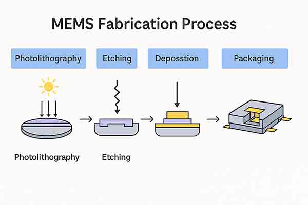
Simplified Fabrication Processes
SOI technology simplifies many aspects of MEMS fabrication compared to approaches using bulk silicon. The buried oxide layer serves multiple functions:
- Acts as a natural etch stop during deep reactive ion etching (DRIE)
- Provides a sacrificial layer for releasing movable structures
- Creates a built-in electrical isolation barrier
- Enables precise control of device layer thickness
- Facilitates wafer bonding processes for complex 3D structures
This multifunctionality reduces the number of processing steps required, potentially lowering manufacturing costs and improving yield. The ability to create suspended structures with well-controlled dimensions is particularly valuable for devices like accelerometers, gyroscopes, and resonators.
Our silicon substrates are available in various specifications to meet the diverse requirements of MEMS fabrication processes, ensuring researchers and manufacturers can access the materials they need for innovative device development.
Key SOI-MEMS Fabrication Techniques
The successful implementation of SOI technology in MEMS devices relies on specialized fabrication techniques that take advantage of the unique structure of SOI wafers. These processes have evolved to enable increasingly complex and precise microstructures.
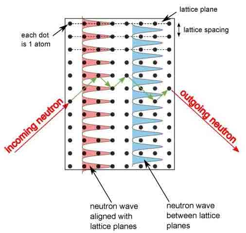
Deep Reactive Ion Etching (DRIE)
Deep Reactive Ion Etching (DRIE) is perhaps the most important fabrication technique for SOI-based MEMS. This process allows for the creation of high-aspect-ratio structures with nearly vertical sidewalls in the silicon device layer. The Bosch process, a common DRIE method, alternates between etching and passivation steps to achieve deep, straight-walled features.
In SOI-MEMS fabrication, the buried oxide layer serves as an excellent etch stop for DRIE, enabling precise control of etch depth. When the etching plasma reaches the buried oxide, the etch rate drops dramatically, effectively halting the vertical progression and ensuring uniform depth across features.
DRIE Process Parameters for SOI-MEMS
- Typical etch rates: 2–10 μm/min
- Aspect ratios: up to 30:1
- Sidewall angles: 89–91°
- Selectivity to oxide: >100:1
- Scallop size: 50–500 nm (process dependent)
- Minimum feature size: ~1–2 μm (standard processes)
- Maximum etch depth: limited primarily by device layer thickness
Sacrificial Layer Release Processes
The buried oxide layer in SOI wafers serves as a natural sacrificial layer for creating suspended MEMS structures. After DRIE patterning of the device layer, the oxide can be selectively removed using wet HF or vapor HF etching to release movable elements. Careful control prevents stiction and ensures complete release, with techniques such as critical point drying and anti-stiction coatings commonly used.
Wafer Bonding Techniques
Advanced SOI-MEMS often incorporate wafer bonding to create complex 3D structures or to encapsulate devices. Common methods include:
- Anodic bonding: Silicon-to-glass bonding at elevated temperature and high voltage, creating hermetic seals.
- Fusion bonding: Direct silicon-to-silicon or silicon-to-oxide bonding, requiring ultra-clean, ultra-flat surfaces and a high-temperature anneal.
- Eutectic bonding: Metal-mediated bonding (e.g., Au–Si) at lower temperatures than fusion bonding.
- Adhesive bonding: Polymer adhesives (e.g., BCB, SU-8) for low-temperature bonding with good mechanical strength.
Silicon nitride (Si₃N₄) coated wafers are often used with SOI for added masking, protection, and dielectric functions in advanced processes.
Innovative SOI-MEMS Sensor Applications
SOI technology has enabled remarkable advancements in MEMS sensor technology, creating devices with unprecedented sensitivity, reliability, and integration capabilities across consumer, industrial, and scientific domains.
Inertial Sensors: Accelerometers and Gyroscopes
SOI-based inertial sensors are ubiquitous in smartphones, wearables, and vehicles. Advantages include superior mechanical properties of single-crystal silicon, excellent electrical isolation, reduced parasitic capacitance, and high-Q resonant structures. Advanced SOI IMUs combine multi-axis sensing with low power consumption and compact packaging.
Pressure Sensors and Microphones
SOI enables miniature, high-precision pressure sensors using thin silicon membranes from the device layer. Tight thickness uniformity ensures consistent mechanical response. Advantages include precise sensitivity control, excellent linearity, low hysteresis, and CMOS compatibility for on-chip conditioning. MEMS microphones fabricated on SOI deliver high SNR and full audio-band response in ultra-compact packages.
Advantages of SOI for Pressure Sensors
- Precise membrane thickness control for tailored sensitivities
- Excellent linearity and low temperature coefficients
- High sensitivity, low hysteresis, and long-term stability
- CMOS-compatible integration of readout and compensation
RF MEMS Components
SOI’s isolation is ideal for RF MEMS—switches, tunable capacitors, resonators, and filters—with low insertion loss, high isolation, and superior linearity. SOI wafers for fast PIN diodes further enhance RF switching performance in communications, satellite, and radar systems.
Key components include low-loss switches, wide-range tunable capacitors, high-Q resonators, and steep-rolloff filters—enabling reconfigurable RF front-ends across crowded spectrums.
Optical MEMS Applications Using SOI
SOI wafers are exceptionally well-suited for MOEMS—devices that manipulate light at the microscale—combining precise mechanical structures with robust optical performance.
Micromirror Arrays and Optical Scanners
SOI enables precise micromirror arrays and scanning systems for DLP projection, optical switching, barcode/LiDAR scanning, adaptive optics, and large optical cross-connects. The BOX layer can act as an optical insulator or reflector depending on thickness and wavelength, enabling interference-based enhancements.
Silicon Photonics Integration
SOI is the standard platform for silicon photonics due to the large index contrast between Si and SiO₂. Combining MEMS actuation with photonic structures yields tunable filters, variable attenuators, optical switches, tunable lasers, and optical phased arrays.
Silicon Photonics Advantages
- Compact circuits with tight optical confinement
- Lower power optical processing
- CMOS-compatible, high-volume fabrication
- Co-integration with control electronics
- Per-channel bandwidths at tens of Gbps
At University Wafer, we provide SOI substrates tailored for photonics (e.g., 220 nm device layers with tight uniformity and low defectivity).
Biomedical Applications of SOI-MEMS
SOI-MEMS enables miniaturized, high-precision sensors and actuators for diagnostic and therapeutic use, with excellent electrical isolation and biocompatibility when properly encapsulated.
Implantable Medical Devices
SOI’s isolation and reliability support implantable pressure sensors, accelerometers, drug delivery systems, neural interfaces, and strain sensors. Proper passivation (Si₃N₄, SiO₂, medical polymers) enables long-term implantation.
Lab-on-Chip and Microfluidic Systems
SOI enables integrated channels, chambers, valves, and sensors with micron-scale precision for point-of-care diagnostics, DNA/protein analysis, cell sorting, drug screening, organ-on-chip, and implantable diagnostics.
SOI-Based Microfluidic Applications
- Rapid, low-volume point-of-care assays
- High-resolution electrophoretic separations
- High-throughput cell sorting/counting
- Parallel drug screening microreactors
- Organ-on-chip platforms for pharma testing
- Chronic implantable diagnostic systems
Our Si₃N₄-coated wafers provide chemical resistance and precise patterning for robust microfluidic devices.
Advanced SOI-MEMS Integration and System-on-Chip Solutions
SOI’s CMOS compatibility enables monolithic integration of mechanical sensors/actuators with electronics, creating compact SoC solutions.
Monolithic Integration Benefits
- Reduced parasitics via direct on-chip connections
- Improved signal integrity and lower noise
- Lower power consumption without off-chip drivers/buffers
- Smaller packages with fewer pins
- Enhanced reliability with fewer interconnects
- Lower total system cost despite higher wafer cost
Integration Challenges and Solutions
- Process compatibility: protect CMOS during MEMS steps
- Thermal budget: keep post-CMOS steps <450 °C
- Contamination control: robust isolation/cleaning protocols
- Mechanical stress: careful layout and stress management
- Design rule alignment: hybrid/compromise rules for MEMS+CMOS
Smart Sensor Systems
Integrated SOI-MEMS enable auto-calibration, self-diagnostics, digital interfaces, multi-sensor fusion, adaptive filtering, and even wireless links—delivering fast, low-power, reliable sensing for Automotive, Industrial, Medical, and Consumer applications.
Future Integration Trends
- AI-enabled sensors with on-chip ML accelerators
- Energy harvesting for self-powered nodes
- Multi-physics sensing on a single die
- Reconfigurable architectures and programmable MEMS
- 3D integration using TSVs for higher density
Our comprehensive SOI wafer services support these trends with specialized substrates and process guidance.
Conclusion
Silicon-On-Insulator (SOI) technology has transformed MEMS, enabling high-performance, highly integrated microsystems that combine mechanical, electrical, and optical functions. Core advantages—electrical isolation, reduced parasitics, precise dimensional control, and excellent mechanical properties—drive innovations across inertial sensing, pressure sensing, RF MEMS, optical MEMS, and biomedical devices.
Key Technology Enablers
- BOX layer: natural etch stop, sacrificial layer, and isolator
- Single-crystal device layer: superior mechanics and reliability
- CMOS compatibility: true monolithic integration
- Precise dimensional control and high yields
- Versatile processes for diverse architectures
With mature DRIE, release, and bonding processes, complex multi-layer MEMS are now manufacturable with high yield. SOI has enabled compact, smart, and power-efficient SoCs, and continues to expand into optical, biomedical, and RF domains. Market growth projections >12% CAGR through 2028 reflect this momentum.
Looking Forward: The Future of SOI-MEMS
Expect deeper integration of AI, energy harvesting, and multi-physics sensing; ultra-thin device layers; novel materials (graphene, piezoelectrics); and 3D stacking. In biomedicine, SOI-MEMS are enabling long-term implantables, lab-on-chip diagnostics, and organ-on-chip systems. The ecosystem—foundries, tools, and materials—has matured to support both R&D and high-volume production.
Our comprehensive SOI wafer solutions provide the substrates and expertise to accelerate innovation from prototype to production.