Float Zone Silicon Wafers for THz Time-Domain Spectroscopy
A PhD in Physics requested a quote for the following:
A peer has forwarded an email from you where you offer certain Si wafers. We would like to order the following items, but we need a formal quote first:
- 2 wafers #C963 — (100) orientation, high-resistivity
- 2 wafers #D092 — (100) orientation, high-resistivity
We need these wafers for our THz time-domain spectroscopy system to block NIR light while transmitting the THz beam.
Reference: #114947 (for specs and pricing)
Accelerate your THz research — request a quote for ultra-high-resistivity silicon and GaAs wafers engineered for maximum transmission and minimal absorption in time-domain spectroscopy.
Order now or request a quote!
Get Your Quote FAST! Or, Buy Online and Start Researching Today!
Our Best-Selling THz Substrates
- High-Resistivity Silicon (FZ) — Optimized for minimal free-carrier absorption in THz-TDS. Resistivity >10,000 Ω·cm. Custom sizes available.
- GaAs (Gallium Arsenide) — High mobility substrates for ultrafast carrier dynamics; semi-insulating and doped options for photoconductive switches.
- Sapphire (Al2O3) — THz-transparent; ideal for optical access and cryogenic experiments.
- InP (Indium Phosphide) — Advanced optoelectronic THz applications; custom thicknesses and orientations.
Why Choose UniversityWafer, Inc.?
- Fast global shipping
- Custom specs for academic and industrial R&D
- Responsive technical support
Additional Request from Customer
Preferred crystal dimensions: 10.0 × 10.0 × 0.2 mm. If unavailable, please quote the smallest wafer in stock. If anti-reflection (AR) coating is offered, the customer requests AR on both larger faces. Otherwise, please recommend an AR-coating vendor. Intended use: terahertz spectroscopy.
Best regards,
Christoph Testud
What Is Terahertz (THz) Spectroscopy?
Terahertz (THz) spectroscopy is a powerful, non-contact technique used to probe the electronic, optical, and structural properties of semiconductors using electromagnetic waves in the terahertz frequency range (0.1 to 10 THz)—which sits between the microwave and infrared regions of the spectrum.

In the context of semiconductors, THz spectroscopy is used to:
🔍 Characterize Carrier Dynamics
- Non-contact measurement of carrier mobility, density, and lifetime.
- THz pulses can excite and then probe the response of free carriers, revealing how they behave in the material over ultrafast timescales (sub-picoseconds to nanoseconds).
⚡ Measure Conductivity
- THz waves are sensitive to changes in conductivity, particularly due to photoexcited carriers (like from a laser pulse).
- This allows researchers to assess photoconductive properties and observe how semiconductors respond under real-time illumination or biasing conditions.
🔬 Investigate Band Structure and Impurities
- THz spectroscopy can detect interband and intraband transitions, especially in narrow-bandgap materials.
- Useful for examining dopant levels, traps, and impurity states in the band gap.
📏 Characterize Thin Films and Nanostructures
- Determine thickness, refractive index, and absorption coefficient of semiconductor films.
- Especially helpful for non-destructive testing of multilayer semiconductor devices.
🧪 Material Identification
- Every semiconductor material has a unique THz spectral “fingerprint” due to lattice vibrations (phonons), making it useful for material verification and defect detection.
THz Time-Domain Spectroscopy (THz-TDS)
One of the most common types, where an ultrashort THz pulse is sent through the semiconductor, and its time delay and attenuation are measured after interacting with the sample. The Fourier transform of this signal gives the complex permittivity and conductivity spectra.

Why It's Valuable:
- Ultrafast (picosecond or femtosecond resolution)
- Non-contact & non-destructive
- Works at low energies (safe for delicate or sensitive materials)
- Can be used at various temperatures, including cryogenic
Example 1: GaAs – Ultrafast Carrier Dynamics
Material: Gallium Arsenide (GaAs)
Why THz? GaAs has high electron mobility, which makes it ideal for high-speed electronics and optoelectronics.
How THz Spectroscopy Helps:
- In pump-probe THz time-domain spectroscopy, a femtosecond laser pulse excites carriers in the GaAs.
- A delayed THz probe pulse detects the photoconductivity and carrier relaxation dynamics.
- Researchers can extract carrier lifetime, mobility, and scattering times, which are critical for optimizing photodetectors, solar cells, or THz emitters.
✅ Result: Allows precise tuning of doping levels, surface passivation layers, and recombination dynamics in high-speed devices.

Example 2: Silicon – Measuring Intrinsic Conductivity and Doping
Material: Intrinsic or lightly doped silicon
Why THz? Silicon is the backbone of modern electronics, and characterizing it non-invasively is very valuable.
How THz Spectroscopy Helps:
- THz-TDS can differentiate doped vs. intrinsic Si by detecting changes in free-carrier absorption.
- THz waves interact with free electrons and holes, and the response varies with dopant type and concentration.
- Useful for quality control of wafers and films, especially when combined with cryogenic or elevated temperature studies.
✅ Result: Non-destructive testing of wafers, evaluation of annealing effects, or verification of SOI (Silicon-On-Insulator) layer uniformity.
🧪 Bonus Application: 2D Materials (e.g., MoS₂, Graphene)
THz spectroscopy is also used to study ultrafast charge transport and plasmonic behavior in 2D materials. Helps in understanding how few-layer materials behave when integrated into next-gen sensors or FETs.
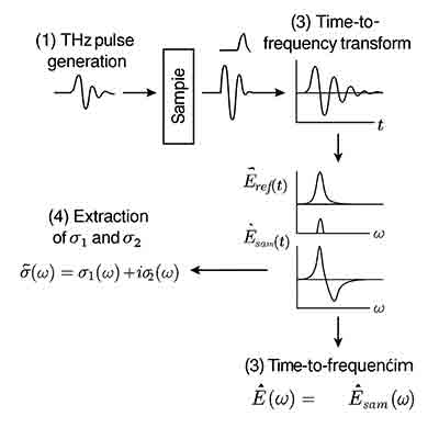
📈 What Is Complex Conductivity?
When a THz pulse interacts with a semiconductor, its amplitude and phase change. From these changes, we can extract the complex conductivity: σ̃(ω) = σ₁(ω) + iσ₂(ω)
Where:
- σ₁(ω) is the real part (represents absorption / energy loss),
- σ₂(ω) is the imaginary part (represents phase shift / energy storage),
- ω is the angular frequency.
⚙️ How It Works: Step-by-Step
- THz-TDS Setup — A femtosecond laser generates an ultrafast optical pulse, which creates a THz pulse via photoconductive antenna or optical rectification. The THz pulse passes through your sample, and a delayed probe pulse measures the transmitted THz field.
- Reference vs. Sample — Measure both: Eref(t) (air) and Esam(t) (sample).
- Fourier Transform — Convert both to frequency domain: Ēref(ω) and Ēsam(ω).
- Transmission Function — Take ratio: T(ω) = Ēsam(ω) / Ēref(ω).
- Extract Material Properties — Compute ε̃(ω) and complex conductivity σ̃(ω) = −iωε₀[ε̃(ω) − 1].
🎯 Why It’s Powerful
- Fast: Probes carrier behavior on sub-picosecond timescales
- Non-contact: No electrodes needed
- Wide spectral range: Ideal for low-energy excitations, phonons, free carriers
- Models: Fit σ̃(ω) with Drude or Drude–Smith to extract mobility, scattering time, and carrier concentration.
Process Overview
- THz pulse generation
- Sample interaction
- Time-to-frequency transform
- Extraction of σ₁ and σ₂