
Supplying Wafers Worldwide Join researchers in over 50 countries.
Call 1-800-713-9375 to connect.
Order today and receive a free consultation from our experts.
Wafer Size Cheat Sheet
- 📏 1″ (25 mm) – rare, early R&D only
- 📏 2″ (50 mm) – MEMS, sensors, photonics
- 📏 3″ (76 mm) – educational, specialty use
- 📏 4″ (100 mm) – still common in university labs
- 📏 6″ (150 mm) – automotive, power electronics
- 📏 8″ (200 mm) – analog, MEMS, IoT chips
- 📏 12″ (300 mm) – CPUs, GPUs, DRAM, NAND
Standard Thicknesses
Thickness increases with wafer diameter:
- 2″ → ~275 µm
- 100 mm (4″) → ~525 µm
- 150 mm (6″) → ~675 µm
- 200 mm (8″) → ~725 µm
- 300 mm (12″) → ~775 µm
Timeline of Wafer Size Evolution
- 1960s → 1″ & 2″ wafers for early ICs
- 1970s → 3″ and 4″ become industry norm
- 1980s → 150 mm (6″) introduced
- 1990s → 200 mm (8″) becomes dominant
- 2000s → 300 mm (12″) mass adoption
- Today → focus on refining 200 & 300 mm, not larger
Handling & Storage Tips
- Always handle wafers by the edge (3 mm margin)
- Use wafer tweezers or vacuum wands — never bare hands
- Store in cassettes for correct size
- Ideal storage: 20–25 °C, 40–60% humidity
- Use cleanroom protocols to prevent contamination
Economic Notes
- Larger wafers → lower cost per chip
- Smaller wafers → more flexibility, less waste
- 200 mm is resurging due to IoT & automotive demand
- 300 mm dominates advanced logic & memory
Explore More
Comparing Silicon Wafer Sizes for Different Projects
Key Takeaways
- Silicon wafer sizes range from 1-inch to 12-inch (300mm), each serving different research and production needs
- Larger wafers (300mm) offer more surface area for chip production but require higher initial investment
- Smaller wafers (2-inch, 5-inch) remain essential for specialized research and small-scale applications
- Wafer selection should consider factors like dopant type, resistivity, and surface finish based on project requirements
- Different manufacturing methods (like Float Zone) impact wafer properties and suitability for specific applications
- Equipment compatibility is a critical factor when selecting wafer sizes for research or production
- Economic considerations should balance initial cost against long-term production efficiency
- Advanced wafer technologies like SOI and epitaxial layers provide enhanced performance for specialized applications
- Proper handling and storage protocols are essential to maintain wafer quality and prevent contamination
- Future trends include continued refinement of existing sizes rather than further diameter increases
Introduction to Silicon Wafer Sizes
Silicon wafers are the foundation for virtually all modern electronic devices, from smartphones to medical equipment. These thin slices of semiconductor material come in various sizes, each with distinct advantages for different applications. Understanding the differences between wafer sizes is crucial for researchers, engineers, and manufacturers to optimize their projects for both performance and cost-efficiency.
The semiconductor industry has evolved significantly since the 1950s, with wafer sizes progressively increasing to improve manufacturing efficiency and reduce costs. Today’s market offers silicon wafers ranging from 1-inch to 12-inch (300mm) diameters, each serving specific needs in the electronics ecosystem.
Silicon wafers are not just uniform discs of silicon; they are precisely engineered substrates with specific properties tailored to their intended applications. The silicon wafer manufacturing process involves multiple steps of purification, crystal growth, slicing, and polishing to achieve the required specifications. Each size category brings its own set of advantages and limitations that must be carefully considered when selecting wafers for a specific project.
The historical progression from smaller to larger wafers has been driven by economics and technological advancement. As semiconductor devices became more complex and miniaturized, larger wafers enabled more efficient production by accommodating more chips per wafer. However, smaller wafers continue to play a vital role in research, specialized applications, and low-volume production scenarios.
The evolution of silicon wafer sizes represents a fascinating mix of technological capability, economic factors, and practical manufacturing considerations. Each increase in diameter has required significant innovations in crystal growth technology, handling equipment, and processing tools. This progression has not been merely about scaling up existing methods but has demanded fundamental advancements in materials science and manufacturing precision.
2-Inch Silicon Wafers: Applications and Specifications
2-inch silicon wafers represent one of the smaller standard sizes available in the semiconductor industry. Despite the industry’s move toward larger wafers for mass production, these compact substrates remain extremely valuable for research, educational purposes, and specialized applications where small batch processing is preferred.

Our 2-inch silicon wafer inventory includes a diverse range of specifications to meet various research and production needs. These wafers are available with different dopant types, including undoped, boron (p-type), gallium (p-type), arsenic (n-type), and antimony (n-type). This variety allows researchers to select the precise electrical properties required for their specific applications.
The primary advantages of 2-inch wafers include:
- Cost-effectiveness: Smaller wafers are more economical for research projects and small-scale production, making them ideal for academic institutions and startups.
- Equipment compatibility: Many research laboratories and educational institutions have equipment designed for 2-inch wafers, making them a practical choice for these settings.
- Lower material waste: When developing new processes or devices, using smaller wafers minimizes material waste during the experimental phase.
- Faster processing times: The smaller surface area means quicker processing times for various fabrication steps, accelerating the research and development cycle.
Typical applications for 2-inch silicon wafers include:
- MEMS (Micro-Electro-Mechanical Systems) device development
- Photonics and optoelectronic research
- Sensor prototyping
- Educational demonstrations and student projects
- Small-scale power device fabrication
For researchers requiring specialized 2-inch wafers, we offer custom specifications with options for resistivity range, thickness, surface finish, and crystal orientation to precisely match project requirements.
The versatility of 2-inch wafers extends beyond traditional semiconductor applications. Their manageable size makes them ideal for emerging fields like bioelectronics, where researchers integrate electronic components with biological systems. Additionally, the lower cost and reduced processing time of these smaller wafers enable more rapid testing in experimental designs, helping innovation in areas such as quantum computing components and novel sensor technologies.
5-Inch and 6-Inch Silicon Wafers: The Mid-Range Options
The 5-inch and 6-inch (150mm) silicon wafer categories represent an important middle ground in the semiconductor industry. These mid-sized wafers strike a balance between the cost-effectiveness of smaller wafers and the production efficiency of larger ones, making them ideal for specific applications and manufacturing scenarios.
Our 5-inch silicon wafers are available in various dopings and types to support both research and production requirements. These wafers provide more usable surface area than 2-inch options while maintaining reasonable costs for medium-scale projects.
The 6-inch (150mm) category, introduced to the semiconductor industry in 1983, has established a significant presence in various applications. Our 150mm silicon wafer inventory includes undoped, boron-doped, and arsenic-doped options to accommodate diverse electronic device requirements.
Key advantages of 5-inch and 6-inch wafers include:
- Optimal for medium-volume production: These sizes provide a good balance between per-wafer cost and production volume capability.
- Equipment availability: Many semiconductor fabrication facilities maintain equipment compatible with these mid-range wafer sizes, making them widely accessible.
- Reduced edge effects: Compared to smaller wafers, the 5-inch and 6-inch options provide more usable area with proportionally less edge area, improving yield for many processes.
- Cost-effective scaling: For projects transitioning from research to limited production, these sizes offer a practical scaling path without the significant investment required for larger wafer processing.
Common applications for 5-inch and 6-inch silicon wafers include:
- Power semiconductors and discrete devices
- Analog integrated circuits
- MEMS devices for automotive and industrial applications
- RF (Radio Frequency) components
- Specialized sensors and detectors
- IoT (Internet of Things) device components
For specialized applications, we can provide custom specifications for both 5-inch and 6-inch wafers, including specific resistivity ranges, thickness tolerances, and surface preparations to meet exact project requirements.
The 6-inch (150mm) wafer size represents a particularly important transition point in semiconductor manufacturing history. It marked the industry’s shift toward more automated handling systems and standardized processing equipment. Many specialty semiconductor manufacturers have optimized their processes specifically for this size, creating a robust ecosystem of tools and techniques. This established infrastructure makes 6-inch wafers particularly valuable for applications like power devices, where the economics and technical requirements don’t necessarily benefit from migration to larger wafer platforms.
8-Inch (200mm) Silicon Wafers: Industrial Standard
The 8-inch (200mm) silicon wafer has established itself as a critical industrial standard in semiconductor manufacturing. Despite the industry’s partial transition to larger wafer sizes, 200mm wafers continue to play a vital role in various applications, particularly for specialized technologies and established manufacturing processes.

The 200mm wafer size represents a significant evolution in semiconductor manufacturing, offering substantial improvements in production efficiency compared to smaller wafers while requiring less capital investment than 300mm fabrication facilities. This size category remains particularly relevant for many semiconductor applications that don’t require the absolute cutting-edge process nodes.
Key advantages of 8-inch silicon wafers include:
- Established manufacturing infrastructure: Many fabrication facilities worldwide are optimized for 200mm production, creating a robust and accessible manufacturing ecosystem.
- Cost-effective for medium-volume production: For many applications, 200mm wafers offer the optimal balance between production volume and capital investment.
- Mature processes: Well-established manufacturing processes for 200mm wafers contribute to high yields and reliable production outcomes.
- Versatility: These wafers support a wide range of device types, from analog and mixed-signal ICs to power semiconductors and MEMS devices.
Common applications for 8-inch silicon wafers include:
- Automotive semiconductors
- Power management ICs
- RF and analog circuits
- Microcontrollers for embedded systems
- MEMS sensors and actuators
- Display drivers
- Specialty memory products
Our 8-inch silicon wafers are available with various specifications, including different resistivity ranges, dopant types, and surface finishes. We can provide both standard and custom specifications to meet specific project requirements, with options for prime-grade, test-grade, or mechanical-grade wafers depending on the application.
For projects requiring enhanced electrical performance, we also offer epitaxial silicon wafers in the 8-inch size, which feature an additional crystalline layer grown on the substrate to provide precise control over electrical properties.
The 8-inch wafer platform has experienced a remarkable comeback in recent years, with global demand exceeding available manufacturing capacity. This resurgence is driven by several factors, including the growth of specialty semiconductor markets like automotive, IoT, and industrial control systems. Additionally, the substantial capital investment required for 300mm facilities has made 200mm manufacturing economically attractive for many applications that don’t require the most advanced process nodes. This has led to significant reinvestment in 200mm capacity worldwide, with both established manufacturers and emerging players expanding their 8-inch fabrication capabilities to meet growing demand.
12-Inch (300mm) Silicon Wafers: Advanced Applications
The 12-inch (300mm) silicon wafer represents the current standard for mainstream semiconductor manufacturing technology. These large-diameter wafers have become the norm for high-volume, advanced node semiconductor production, enabling the creation of cutting-edge processors, memory, and other complex integrated circuits.
Our 300mm silicon wafers are designed for microelectronic device production at the highest level of precision. These wafers feature exceptional specifications, including thickness tolerance of ±0.1 micron and orientation accuracy of ±2 degrees, ensuring optimal performance for demanding applications.
The primary advantages of 12-inch silicon wafers include:
- Maximum production efficiency: With 2.25 times the surface area of 200mm wafers, 300mm wafers significantly increase the number of chips that can be produced per wafer, reducing the per-chip manufacturing cost.
- Advanced process compatibility: Most leading-edge semiconductor manufacturing processes (7nm, 5nm, and beyond) are developed and optimized for 300mm wafers.
- Superior uniformity: Larger wafers typically demonstrate better process uniformity across the surface, improving yield for complex devices.
- Reduced edge waste percentage: The ratio of edge area (which often has defects or incomplete devices) to total wafer area is lower for 300mm wafers, improving overall yield.
Our 12-inch silicon wafer inventory includes prime-grade options with P-type/Boron doping, meeting precise diameter specifications of 299.8 to 300.2mm. These wafers are not reclaimed but new, ensuring the highest quality for critical applications.
Common applications for 300mm silicon wafers include:
- Advanced microprocessors and SoCs (Systems on Chip)
- High-density memory (DRAM, NAND Flash)
- High-performance GPUs (Graphics Processing Units)
- AI and machine learning accelerators
- Advanced mobile application processors
- Server and data center chips
For specialized research needs, we can provide custom specifications on 300mm wafers, including specific resistivity ranges, crystal orientations, and surface preparations to meet the exact requirements of advanced research and development projects.
The transition to 300mm wafers represented a major milestone in semiconductor manufacturing history, requiring unprecedented collaboration among equipment suppliers, wafer manufacturers, and chip producers. This shift involved not just scaling up existing technologies but developing entirely new approaches to crystal growth, wafer handling, and process control. The 300mm platform introduced higher levels of automation and standardization, significantly reducing human handling and associated contamination risks. These innovations have enabled the production of devices with billions of transistors at increasingly smaller geometries, supporting the continued advancement of computing power, memory density, and energy efficiency that drives modern digital technology.
Specialized Silicon Wafer Types: Float Zone and SOI
Beyond standard silicon wafers, specialized types like Float Zone (FZ) and Silicon on Insulator (SOI) wafers offer unique properties for specific applications. These advanced substrates provide enhanced performance characteristics that make them ideal for specialized electronic devices and research applications.
Float Zone Silicon Wafers
Our Float Zone silicon wafers are manufactured using a specialized process that produces extremely high-purity silicon. The Float Zone method involves melting a narrow region of a silicon rod using radio frequency heating, with the molten zone moving along the rod to redistribute impurities and create a highly pure crystal structure.
Key characteristics of Float Zone wafers include:
- Ultra-high resistivity: FZ wafers can achieve resistivity values exceeding 10,000 Ohm-cm, making them ideal for high-voltage applications and sensitive detectors.
- Minimal oxygen content: The FZ process avoids contact with crucible materials, resulting in very low oxygen concentration compared to Czochralski-grown wafers.
- Low defect density: The crystal quality of FZ wafers is exceptionally high, with minimal dislocations and other crystallographic defects.
- Superior minority carrier lifetime: The high purity of FZ silicon results in longer carrier lifetimes, enhancing the performance of certain electronic devices.
Our Float Zone silicon wafer inventory includes options like 2-inch diameter, 1,000±25µm thickness, intrinsic undoped Si with [100]±0.5° orientation, and resistivity exceeding 10,000 Ohm-cm. These wafers are available with both-sides-polished finish for optimal surface quality.
The exceptional purity of Float Zone silicon makes it particularly valuable for high-performance detectors, including radiation detectors for scientific research and medical imaging applications. The ultra-high resistivity and long carrier lifetime enable superior signal-to-noise ratios and detection sensitivity. Additionally, the low oxygen content makes FZ wafers ideal for devices operating in extreme environments, such as high-radiation settings or applications requiring exceptional thermal stability. While more costly than standard Czochralski wafers, the unique properties of Float Zone silicon enable performance capabilities that cannot be achieved with conventional materials.
Silicon on Insulator (SOI) Wafers
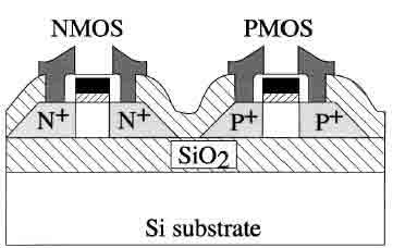
Silicon on Insulator (SOI) wafers feature a layered structure with a thin silicon layer bonded to an insulating substrate, typically silicon dioxide (SiO2). This configuration offers significant advantages for certain applications by providing electrical isolation between the device layer and the substrate.
Key benefits of SOI wafers include:
- Reduced parasitic capacitance: The insulating layer minimizes capacitive coupling to the substrate, improving high-frequency performance.
- Better isolation: SOI structures provide superior electrical isolation between adjacent devices, reducing crosstalk and enabling higher integration density.
- Improved radiation hardness: The insulating layer helps protect devices from radiation-induced effects, making SOI wafers valuable for aerospace and nuclear applications.
- Lower power consumption: SOI-based devices typically operate at lower power levels due to reduced leakage currents and parasitic capacitances.
- Enhanced high-temperature performance: The isolation layer improves device performance at elevated temperatures by reducing leakage currents.
SOI wafers are particularly valuable for applications including RF circuits, high-temperature electronics, radiation-hardened devices, and advanced CMOS (Complementary Metal-Oxide-Semiconductor) technologies. We offer various SOI wafer specifications with different device layer thicknesses, buried oxide thicknesses, and resistivity values to meet specific project requirements.
The evolution of SOI technology has been driven by increasingly demanding performance requirements in multiple semiconductor sectors. Modern SOI manufacturing techniques include bonded SOI, SIMOX (Separation by Implantation of Oxygen), and Smart Cut™ processes, each offering different advantages for specific applications. The enhanced performance of SOI-based devices has made them particularly valuable in applications where power efficiency, speed, and reliability are paramount, such as server processors, automotive electronics, and aerospace systems. As device scaling becomes more challenging, SOI technologies continue to gain importance by providing alternative pathways to performance improvement beyond traditional dimensional scaling.
Wafer Selection Guide: Matching Size to Project Requirements
Selecting the appropriate silicon wafer size for your project involves considering multiple factors beyond just diameter. This comprehensive guide will help you navigate the selection process to ensure you choose the optimal wafer specifications for your specific application.
Project Scale Considerations
The scale of your project is a primary factor in wafer size selection:
- Research and Prototyping: For early-stage research, academic projects, or initial prototyping, smaller wafers (2-inch to 4-inch) are typically most cost-effective. These sizes minimize material costs while allowing for process development and concept validation.
- Small to Medium Production: For limited production runs or specialized applications with moderate volume requirements, 5-inch to 8-inch (150mm to 200mm) wafers often provide the optimal balance between cost and manufacturing efficiency.
- High-Volume Manufacturing: For mass production of commercial devices, particularly those requiring advanced process nodes, 12-inch (300mm) wafers deliver the greatest economies of scale and are compatible with leading-edge fabrication facilities.
Equipment Compatibility
Existing fabrication equipment places significant constraints on wafer size selection:
- Academic and Research Labs: Many university and small research facilities are equipped for 2-inch to 4-inch wafers, making these sizes practical choices for academic research.
- Established Fabs: Many semiconductor fabrication facilities are optimized for specific wafer sizes (commonly 6-inch, 8-inch, or 12-inch), and changing sizes may require substantial equipment modifications or replacements.
- Service Providers: When using external fabrication services, it’s important to verify which wafer sizes they support for your specific process requirements.
Application-Specific Factors
Different applications have unique requirements that influence wafer size selection:
- Device Complexity: More complex devices with smaller feature sizes typically benefit from larger wafers with better uniformity across the surface.
- Yield Sensitivity: Applications with high yield sensitivity may benefit from larger wafers that offer more consistent processing across the surface.
- Cost Constraints: Budget-sensitive projects should carefully balance the higher per-wafer cost of larger diameters against the improved production efficiency they provide.
- Thermal Considerations: Some high-power or high-temperature applications may have specific requirements regarding wafer thickness and thermal properties that vary with wafer size.
Our technical support team is available to help you navigate these considerations and select the optimal wafer specifications for your project. We offer free silicon wafer support on all substrates, ensuring you receive the right materials for your specific application requirements.
When selecting wafers for specialized research applications, it’s important to consider not just the current experimental phase but also potential scaling requirements for future development. A project that begins in a research setting may eventually need to transition to pilot production and beyond. Planning this pathway early can prevent complications when scaling up. Additionally, the availability of analytical data for specific wafer types can be valuable—some wafer specifications have more extensive characterization in the scientific literature, providing a stronger foundation for comparison and validation of research results. Our technical team can provide guidance on selecting wafers with well-documented properties that align with both your immediate research needs and potential future development paths.
Economic Considerations: Cost vs. Efficiency
The economics of silicon wafer selection involves balancing initial costs against long-term efficiency gains. Understanding this relationship is crucial for optimizing project budgets while meeting technical requirements.

Cost Structure Analysis
The cost structure for silicon wafers includes several components that vary with wafer size:
- Per-Wafer Price: Larger wafers have higher unit costs due to the increased silicon material, more demanding manufacturing processes, and tighter specifications required for larger diameters.
- Die Yield Considerations: While larger wafers cost more per unit, they yield proportionally more dies. A 300mm wafer provides approximately 2.25 times the surface area of a 200mm wafer, potentially yielding more than twice as many chips.
- Processing Costs: Many processing steps (such as lithography, etching, and deposition) have costs that scale less than linearly with wafer area, making larger wafers more economical on a per-die basis.
- Equipment Investment: Transitioning to larger wafer sizes typically requires significant capital investment in new processing equipment, which must be amortized across production volume.
Optimizing for Different Project Types
Different project categories benefit from different economic approaches:
- Research Projects: For research applications, minimizing total project cost is often the priority. Smaller wafers (2-inch to 4-inch) typically offer the lowest absolute cost and greatest flexibility, making them ideal for experimental work where multiple iterations may be required.
- Small-Batch Production: For limited production runs, mid-sized wafers (5-inch to 8-inch) often provide the best balance between setup costs, processing efficiency, and total material investment.
- High-Volume Manufacturing: For mass production, the per-die cost efficiency of 300mm wafers typically outweighs their higher unit price, especially for advanced node devices where yield and uniformity are critical.
Practical Cost-Saving Approaches
We offer several options to help optimize costs while meeting technical requirements:
- Partial Cassette Purchases: Our flexible purchasing options allow buying as few as one wafer, eliminating the need to purchase full cassettes when only a small quantity is required.
- Test Grade Options: For applications that don’t require prime-grade specifications, test-grade wafers can provide significant cost savings while meeting functional requirements.
- Reclaimed Wafers: For certain applications, reclaimed wafers (previously used and repolished) offer substantial cost savings with minimal impact on performance.
- Custom Specifications: By specifying only the critical parameters for your application rather than overspecifying, you can often achieve significant cost savings without compromising functionality.
Our team provides free technical assistance to help you optimize wafer selection for both technical performance and cost efficiency, ensuring your project achieves the best possible balance between these factors.
The economic analysis of wafer selection should also consider hidden costs that may not be immediately apparent. For instance, larger wafers typically require more sophisticated handling equipment and stricter environmental controls, potentially increasing facility costs. Similarly, the risk profile differs across wafer sizes—a processing error on a 300mm wafer represents a larger financial loss than on a smaller wafer. For research institutions and startups with limited funding, the ability to purchase smaller quantities of smaller wafers allows for more experimental iterations within a fixed budget. Conversely, high-volume manufacturers must consider not just the direct wafer costs but also factors like throughput capacity, equipment utilization rates, and facility overhead allocation, which often favor larger wafer sizes despite their higher unit costs.
Advanced Wafer Technologies: Epitaxial, SOI, and Beyond
Beyond standard silicon wafers, advanced substrate technologies offer enhanced performance characteristics for specialized applications. These engineered wafers feature modified structures or additional layers that provide specific benefits for particular device types.
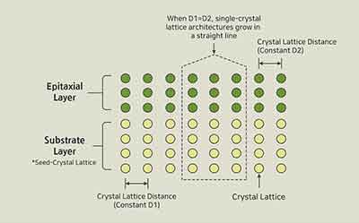
Epitaxial Silicon Wafers
Epitaxial silicon wafers feature an additional crystalline silicon layer grown on top of the silicon substrate. This epitaxial layer has precisely controlled electrical properties that may differ from those of the underlying substrate, enabling optimized device performance.
Key advantages of epitaxial wafers include:
- Precise Dopant Control: The epitaxial layer can have very precisely controlled dopant concentration and distribution, independent of the substrate.
- Buried Layer Functionality: Epitaxial structures can incorporate buried layers with specific electrical properties, enabling advanced device architectures.
- Defect Reduction: The epitaxial growth process can reduce certain types of crystalline defects, improving device performance and yield.
- Enhanced Latch-up Immunity: For CMOS devices, epitaxial structures can provide improved latch-up immunity compared to standard wafers.
Common applications for epitaxial wafers include power devices, bipolar transistors, BiCMOS (Bipolar-CMOS) integrated circuits, and various analog devices where precise control of electrical parameters is critical.
Silicon on Insulator (SOI) Technology
Silicon on Insulator (SOI) technology incorporates an insulating layer (typically silicon dioxide) between the device layer and the substrate. This configuration offers significant advantages for many applications by electrically isolating the active device region.
Key benefits of SOI technology include:
- Reduced Parasitic Effects: The insulating layer minimizes parasitic capacitances and leakage currents, improving device performance.
- Enhanced High-Frequency Operation: SOI structures enable better high-frequency performance due to reduced substrate coupling effects.
- Improved Radiation Hardness: The insulating layer provides inherent protection against certain radiation-induced effects, making SOI valuable for aerospace and nuclear applications.
- Lower Power Consumption: SOI-based devices typically operate with lower power requirements due to reduced capacitive loading and leakage.
SOI wafers are available in various configurations, including:
- SIMOX (Separation by Implantation of Oxygen): Created by oxygen implantation followed by high-temperature annealing.
- Bonded SOI: Formed by bonding two wafers with an oxide layer and thinning one to create the device layer.
- Smart Cut™: A specialized process combining implantation and bonding to create precisely controlled SOI structures.
Ultra-Thin Wafers
Ultra-thin silicon wafers, with thicknesses ranging from a few microns to less than 100 microns, enable specialized applications where standard wafer thicknesses (typically 500-750 microns) are unsuitable. These extremely thin substrates are particularly valuable for applications requiring flexibility, improved thermal characteristics, or 3D integration.
Key applications for ultra-thin wafers include:
- 3D Integration: Stacking of multiple thin device layers to create high-density 3D integrated circuits.
- Flexible Electronics: Ultra-thin silicon enables creation of flexible or conformable electronic devices.
- Improved Thermal Management: Thinner substrates can provide better heat dissipation for high-power devices.
- Through-Silicon Vias (TSVs): Ultra-thin wafers facilitate the creation of TSVs for advanced packaging technologies.
We offer a variety of advanced wafer technologies in different size formats, allowing you to select the optimal combination of wafer diameter and specialized structure for your specific application requirements.
Advanced wafer technologies continue to evolve rapidly to address emerging application requirements. For instance, strained silicon technology, which introduces tensile or compressive strain in the crystal lattice to enhance carrier mobility, has become increasingly important for high-performance devices. Similarly, silicon-germanium (SiGe) epitaxial layers enable band gap engineering for improved device characteristics. More exotic structures like silicon-on-nothing (SON), where a void is created beneath the device layer, and cavity SOI, featuring embedded air gaps for enhanced isolation, represent the cutting edge of substrate engineering. These specialized substrates enable device designers to overcome fundamental physical limitations and continue advancing performance even as traditional dimensional scaling becomes more challenging.
Surface Finishes and Processing Options
The surface finish of a silicon wafer significantly impacts its suitability for specific applications and processes. Different surface preparations offer varying advantages for particular fabrication techniques and device types.
Standard Surface Finish Options
Our silicon wafers are available with several standard surface finish options:
- Single-Side Polished (SSP): These wafers have one side polished to a mirror-like finish while the other side remains etched or lapped. SSP wafers are suitable for applications where only one side requires a high-quality surface, such as certain sensor applications or when backside metallization will be applied.
- Double-Side Polished (DSP): Both sides of DSP wafers are polished to a high-quality finish. These wafers are ideal for applications requiring processing on both surfaces or for devices that need excellent flatness and parallelism, such as MEMS devices or through-wafer processing.
- Chemical-Mechanical Polished (CMP): This specialized polishing technique combines chemical etching with mechanical abrasion to achieve extremely smooth surfaces with minimal subsurface damage. CMP finishes are particularly important for advanced lithography processes with small feature sizes.
- Epitaxial Ready: These wafers undergo specialized cleaning and preparation to ensure they’re optimized for epitaxial layer growth, with minimal surface contamination or defects that could interfere with the epitaxial process.
Surface Roughness Specifications
Surface roughness is typically specified using Ra (average roughness) or RMS (root mean square) values, measured in angstroms (Å) or nanometers (nm). Common specifications include:
- Ultra-Smooth: <0.5nm RMS, suitable for advanced lithography and nanoscale devices
- Standard Polish: 0.5-1nm RMS, appropriate for most microelectronic applications
- Mechanical Polish: 1-5nm RMS, suitable for less demanding applications
The appropriate surface roughness specification depends on the minimum feature size of your devices and the specific processes you’ll be using. Our technical team can help you select the optimal surface finish specification for your particular application.
Special Surface Treatments
Beyond standard polishing, we offer specialized surface treatments for specific applications:
- Thermal Oxide Layers: Pre-grown silicon dioxide layers of specified thicknesses for immediate device processing
- Nitride Coatings: Silicon nitride layers for specialized applications requiring this surface chemistry
- Metal Coatings: Various metallization options including aluminum, gold, titanium, and others
- Patterned Wafers: Pre-patterned surfaces with alignment marks or test structures
Custom Surface Specifications
For specialized applications, we can provide custom surface preparations according to your exact requirements. These may include:
- Specific Roughness Values: Tailored surface roughness specifications for particular device types
- Special Cleaning Protocols: Enhanced cleaning procedures for ultra-sensitive applications
- Custom Edge Treatments: Specialized edge rounding or beveling to reduce edge defects
- Surface Activation: Chemical treatments to prepare surfaces for specific bonding or deposition processes
Our technical support team can work with you to determine the optimal surface finish and any special processing requirements for your specific application, ensuring you receive wafers that are ideally suited to your fabrication process and device specifications.
The impact of surface finish on device performance extends beyond mere topographical considerations. Surface chemistry plays a crucial role in many applications, particularly those involving interfaces or surface interactions. For instance, hydrophilic surfaces (typically achieved through specific cleaning processes) facilitate wafer bonding, while hydrophobic surfaces may be preferable for certain deposition processes. Surface microroughness can significantly influence carrier mobility in channel regions of transistors, while nanoscale surface features can affect optical properties in photonic applications. Advanced characterization techniques like X-ray photoelectron spectroscopy (XPS) and atomic force microscopy (AFM) allow precise evaluation of surface properties beyond traditional parameters. For cutting-edge applications, we can provide detailed surface characterization data to ensure compatibility with specific process requirements.
Wafer Handling, Storage, and Safety Considerations
Proper handling, storage, and safety protocols are essential when working with silicon wafers to maintain their quality, prevent contamination, and ensure workplace safety. These considerations become increasingly important as wafer size increases, with larger wafers requiring more careful handling due to their increased fragility and value.
Wafer Handling Best Practices
To maintain wafer integrity and prevent contamination, follow these handling guidelines:
- Use Appropriate Tools: Always use vacuum wands, wafer tweezers, or other specialized tools designed for wafer handling. Never touch wafers directly with bare hands.
- Handle by the Edge: When manual handling is necessary, only touch the outer edge of the wafer (preferably within 3mm of the edge) to avoid contaminating or damaging the active surface area.
- Minimize Exposure Time: Keep wafers in their protective containers whenever they’re not being processed to minimize exposure to airborne contaminants.
- Clean Room Protocols: Follow clean room protocols appropriate for your wafer type and application, including proper gowning, air shower use, and material transfer procedures.
- Movement Precautions: Move wafers slowly and deliberately to avoid generating particles through rapid air movement or static discharge.
Storage Requirements
Proper storage is essential for maintaining wafer quality over time:
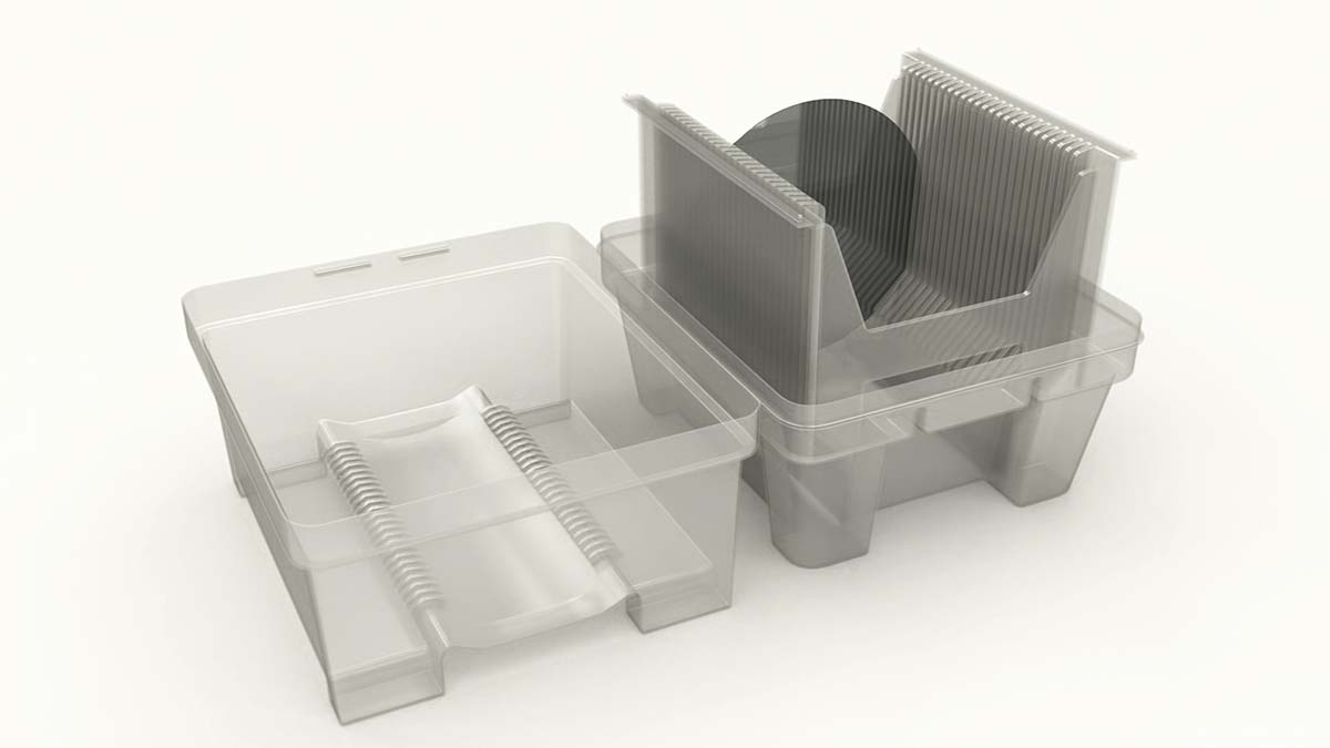
- Cassette Storage: Store wafers in appropriate cassettes or carriers designed for their specific diameter. Our wafer cassettes are designed to protect wafers from physical damage and contamination.
- Environmental Control: Maintain appropriate temperature, humidity, and air quality in storage areas. Ideal conditions typically include:
- Temperature: 20-25°C (68-77°F)
- Relative humidity: 40-60%
- Filtered air to minimize particulate contamination
- Packaging Materials: Use only clean, lint-free, non-outgassing materials for any packaging that contacts wafers.
- Inventory Management: Implement proper inventory management with FIFO (First In, First Out) protocols to ensure wafers don’t remain in storage unnecessarily long.
Safety Considerations
Silicon wafers present several safety considerations that should be addressed:
- Physical Hazards: Wafers can break into extremely sharp fragments. Always wear appropriate cut-resistant gloves when handling wafers, especially broken ones.
- Chemical Exposure: Some wafer types may have residual chemicals from processing. Review the Material Safety Data Sheet (MSDS) for any specific handling precautions.
- Ergonomic Considerations: Implement proper ergonomic practices for wafer handling to prevent repetitive strain injuries, particularly when handling multiple wafers.
- Disposal Protocols: Follow appropriate disposal protocols for broken or used wafers, which may be classified as industrial waste in some jurisdictions.
Transportation Considerations
When transporting wafers between facilities or shipping to customers, special precautions are necessary:
- Specialized Containers: Use shipping containers specifically designed for semiconductor wafers, with appropriate cushioning and support.
- Shock Indicators: Consider using shock and tilt indicators on shipments to monitor for potentially damaging handling during transit.
- Climate Control: For sensitive wafers, use climate-controlled shipping methods to prevent temperature or humidity extremes.
- Proper Labeling: Ensure packages are clearly labeled as fragile electronic components to encourage appropriate handling.
Our same-day shipping in Boston and next-day delivery nationwide services are designed with these considerations in mind, ensuring your wafers arrive quickly and in optimal condition.
The electrostatic properties of silicon wafers present additional handling challenges that require specific precautions. Silicon wafers can develop significant electrostatic charges during handling, which can attract contaminating particles or potentially damage sensitive device structures. Proper grounding of personnel and equipment is essential, particularly in low-humidity environments where static buildup is more pronounced. Ionized air systems are often employed in critical handling areas to neutralize static charges. For particularly sensitive applications, such as those involving nanoscale structures or specialized coatings, customized handling protocols may be necessary. Our packaging and shipping methods incorporate appropriate electrostatic discharge (ESD) protection measures, including antistatic materials and humidity control, to preserve wafer integrity throughout the transportation process.
Future Trends in Silicon Wafer Technology
The silicon wafer industry continues to evolve in response to changing semiconductor manufacturing requirements and emerging technologies. Understanding these trends can help researchers and manufacturers prepare for future developments and make informed decisions about current investments.
Evolution of Wafer Sizes
The historical progression of wafer sizes has been driven by economic factors, with each increase in diameter enabling more efficient production:
- Historical Progression: From the 1-inch wafers of the 1960s to today’s 300mm (12-inch) standard, wafer diameters have increased to improve manufacturing economics.
- 450mm Development Status: While 450mm (18-inch) wafer development has been explored, the industry has largely concluded that the capital investment required does not justify the benefits for most applications. The focus has shifted toward optimizing 300mm manufacturing and exploring alternative approaches to cost reduction.
- Specialty Size Growth: Renewed interest in specialty wafer sizes (particularly 200mm) for automotive, IoT, and industrial applications reflects the diversification of semiconductor markets.
Advanced Materials and Structures
Several technological trends are shaping the future of silicon wafer technology:
- Engineered Substrates: Increasing use of engineered substrates like SOI, strained silicon, and silicon-germanium to enhance device performance beyond traditional scaling.
- Heterogeneous Integration: Growing demand for substrates that support heterogeneous integration of different materials and device types on the same wafer.
- 3D Integration Technologies: Ultra-thin wafers and through-silicon via (TSV) technologies enabling vertical integration of multiple device layers.
- New Crystal Orientations: Exploration of non-standard crystal orientations to optimize specific device properties, particularly for emerging applications.
Manufacturing Innovation
Continuous improvements in wafer manufacturing processes are driving quality enhancements:
- Defect Reduction: Advanced crystal growth techniques and improved quality control methods are reducing defect densities to unprecedented levels.
- Uniformity Improvements: Enhanced process control is enabling better thickness uniformity, flatness, and electrical parameter consistency across wafers.
- Sustainability Focus: Industry emphasis on reducing energy consumption, water usage, and waste generation in wafer manufacturing processes.
- Automation and AI Integration: Implementation of artificial intelligence and machine learning to optimize manufacturing processes and predict quality issues.
Market Trends
Several market trends are influencing wafer technology development:
- Automotive Electronics Growth: Increasing demand for automotive-grade wafers with enhanced reliability specifications and temperature ratings.
- IoT Device Requirements: Need for cost-effective wafers optimized for low-power, high-volume IoT applications.
- Power Electronics Evolution: Growing adoption of wide bandgap materials like silicon carbide and gallium nitride for power applications, complementing rather than replacing silicon.
- Edge Computing Demands: Requirements for specialized wafers optimized for edge computing and AI acceleration applications.
At University Wafer, we continue to monitor these trends and adapt our offerings to meet evolving customer requirements. Our technical team stays current with industry developments to provide guidance on selecting wafer technologies that will support both current needs and future scalability.
Conclusion
Silicon wafer selection is a critical decision that impacts project success, cost-effectiveness, and long-term scalability. Understanding the characteristics and applications of different wafer sizes—from 2-inch research wafers to 300mm production substrates—enables informed decision-making that optimizes both technical performance and economic outcomes.
The choice between wafer sizes depends on multiple interconnected factors including project scale, equipment compatibility, application requirements, and budget constraints. Smaller wafers (2-inch to 4-inch) remain valuable for research, prototyping, and specialized applications where cost-effectiveness and flexibility are paramount. Mid-sized wafers (5-inch to 8-inch) provide optimal balance for medium-volume production and established manufacturing processes. Large wafers (300mm) deliver maximum efficiency for high-volume production of advanced devices.
Advanced wafer technologies including Float Zone, SOI, epitaxial, and ultra-thin variants expand the possibilities for specialized applications requiring enhanced performance characteristics. These engineered substrates enable device capabilities that cannot be achieved with standard wafers, supporting continued advancement in electronics performance.
Economic considerations must balance initial wafer costs against long-term production efficiency, equipment requirements, and market demands. The resurgence of certain wafer sizes, particularly 200mm for automotive and IoT applications, demonstrates that the “bigger is always better” paradigm has evolved into a more nuanced understanding of optimal sizing for specific market segments.
Future trends suggest continued refinement of existing wafer sizes rather than dramatic increases in diameter. The focus has shifted toward advanced materials, specialized structures, improved manufacturing processes, and sustainability initiatives. These developments promise enhanced performance capabilities while addressing the diverse requirements of emerging technology sectors.
At University Wafer, we provide comprehensive silicon wafer solutions across all standard sizes and specialized variants. Our technical expertise and flexible supply options ensure that researchers and manufacturers can access the precise wafer specifications needed for their projects, whether for initial research, pilot production, or high-volume manufacturing. The continued evolution of silicon wafer technology promises exciting possibilities for advancing electronic device performance and enabling new applications across diverse industries.